Toyota G9200 Inverter: Difference between revisions
Malvineous (talk | contribs) (Add CSIG schematic from xp677) |
Malvineous (talk | contribs) (Add CSI (clocked serial) information) |
||
| Line 14: | Line 14: | ||
| 2904Z<br/>A126G<br/>JRC || JRC || JRC2904 || Dual op-amp | | 2904Z<br/>A126G<br/>JRC || JRC || JRC2904 || Dual op-amp | ||
|- | |- | ||
| 76F0080GC || Renesas/NEC || 76F0018 || [[wikipedia:V850|V850 series microcontroller]]. "Special Customer Version", appears to be closest in specs to V850E/CA1 model. Two on the logic board, perhaps one each for MG1 and MG2. Supported by GCC in "v850" architecture. | | 76F0080GC || Renesas/NEC || 76F0018 || [[wikipedia:V850|V850 series microcontroller]]. "Special Customer Version", appears to be closest in specs to V850E/CA1 model. Two on the logic board, perhaps one each for MG1 and MG2. Supported by GCC in "v850" architecture. Datasheets available at [https://www.renesas.com/us/en/products/microcontrollers-microprocessors/other-mcus-mpus/v850-family-mcus?field-lead-cnt=100&method-field-lead-cnt=OR Renesas]. The exact model is unknown, but select one that is 14 × 14mm with 100 pins. | ||
|- | |- | ||
| VHC<br/>32-S<br/>D1 31 || ? || 74VHC32 || Quad 2-input OR gate | | VHC<br/>32-S<br/>D1 31 || ? || 74VHC32 || Quad 2-input OR gate | ||
|- | |- | ||
| 9N25<br/>SE617<br/><u>D</u> <hr/> 4M27<br/>SE617<br/><u>D</u> || Denso || SE617 || | | 9N25<br/>SE617<br/><u>D</u> <hr/> 4M27<br/>SE617<br/><u>D</u> || Denso || SE617 || Single/differential transceiver. Used to convert the CSI (clocked serial) signals (CLK/MTH/HTM) to/from +/- differential pairs, as the NEC V850 CPU only outputs a single-ended signal, and the differential pair extends this signal outside the inverter to communicate with the other ECUs. | ||
|- | |- | ||
| 9N29<br/>SE874<br/><u>D</u>G || Denso? || SE874 || Main interface IC? Only one on the board. Possible switching power supply control IC. | | 9N29<br/>SE874<br/><u>D</u>G || Denso? || SE874 || Main interface IC? Only one on the board. Possible switching power supply control IC. | ||
| Line 228: | Line 228: | ||
Image:Toyota G9200 inverter schematic - SE617.png|SE617 MTH/HTM CSIG I/O schematic | Image:Toyota G9200 inverter schematic - SE617.png|SE617 MTH/HTM CSIG I/O schematic | ||
</gallery> | </gallery> | ||
== Interfaces == | |||
=== Clocked Serial Interface (CSI) === | |||
The two NEC V850 CPUs on board both support Clocked Serial Interfaces (CSI). All interfaces on the chip are tagged alphabetically, and the CSI interfaces are tagged "G", so the datasheet refers to this as CSIG. | |||
The inverter uses the CSI interface to communicate with the outside world, via Denso SE617 differential transceivers. These convert the single-ended signal line into two signals (a positive and negative version) which is better suited to noise rejection and can be sent outside the inverter. | |||
See [[Toyota Inverter Clocked Serial Interface Protocol]] for details on the data sent over these interfaces. | |||
[[Category:Toyota G9200]] | [[Category:Toyota G9200]] | ||
[[Category:Toyota]] | [[Category:Toyota]] | ||
[[Category:Inverter]] | [[Category:Inverter]] | ||
Revision as of 02:41, 26 February 2023
The Toyota G9200 series of inverters was used on a number of vehicles, including the third generation Prius.
ICs
| Markings | Manufacturer | Model | Purpose |
|---|---|---|---|
| 074Z 1069B JRC |
JRC | NJM074 | Quad J-FET input op-amp |
| 2901Z 10458 JRC |
JRC | JRC2901 NJM2901 |
Single-supply quad comparator |
| 2903Z 10696 JRC |
JRC | JRC2903 | Single-supply dual voltage comparator |
| 2904Z A126G JRC |
JRC | JRC2904 | Dual op-amp |
| 76F0080GC | Renesas/NEC | 76F0018 | V850 series microcontroller. "Special Customer Version", appears to be closest in specs to V850E/CA1 model. Two on the logic board, perhaps one each for MG1 and MG2. Supported by GCC in "v850" architecture. Datasheets available at Renesas. The exact model is unknown, but select one that is 14 × 14mm with 100 pins. |
| VHC 32-S D1 31 |
? | 74VHC32 | Quad 2-input OR gate |
| 9N25 SE617 D 4M27 SE617 D |
Denso | SE617 | Single/differential transceiver. Used to convert the CSI (clocked serial) signals (CLK/MTH/HTM) to/from +/- differential pairs, as the NEC V850 CPU only outputs a single-ended signal, and the differential pair extends this signal outside the inverter to communicate with the other ECUs. |
| 9N29 SE874 DG |
Denso? | SE874 | Main interface IC? Only one on the board. Possible switching power supply control IC. |
| AU6801N1 | Tamagawa | Smartcoder AU6802N1 | Resolver decoders, two on the logic board underside. Likely connected to D29 to sense MG1 and MG2 rotor angle. |
Connectors
This section lists the connectors found on the original factory inverter and where known, the purpose and characteristics of each pin in the connector.
A59 (Control signals)

| Identifier | Pin | Name | Connects from | Purpose |
|---|---|---|---|---|
| A59-1 | 1 | IGCT | Junction connector A55-11, then Power Management Control ECU pins A21-2 and A22-5 | ? |
| A59-2 | 2 | IDH | A/C Amplifier Assembly L17-27 | ? |
| A59-3 | 3 | VLO | Power Management Control ECU pin A21-11 | Unknown. When power switch on, should be below 1 V. |
| A59-4 | 4 | - | ||
| A59-5 | 5 | CLK+ | Power Management Control ECU pin A22-21 | ? |
| A59-6 | 6 | REQ+ | Power Management Control ECU pin A22-33 | ? |
| A59-7 | 7 | MTH+ | Power Management Control ECU pin A22-30 | ? |
| A59-8 | 8 | HTM+ | Power Management Control ECU pin A22-24 | ? |
| A59-9 | 9 | +B2 | A59-10 (+B) | Backup for pin A59-10 |
| A59-10 | 10 | +B | A59-9, and 12 V battery via 10 A fuse and IGCT relay, switched by Power Management Control ECU pin MREL | ? |
| A59-11 | 11 | S | 12 V battery via 5 A fuse | ? |
| A59-12 | 12 | NODD | Power Management Control ECU pin A21-21 | Inverter disable |
| A59-13 | 13 | - | ||
| A59-14 | 14 | - | ||
| A59-15 | 15 | CLK- | Power Management Control ECU pin A22-20 | ? |
| A59-16 | 16 | REQ- | Power Management Control ECU pin A22-32 | ? |
| A59-17 | 17 | MTH- | Power Management Control ECU pin A22-29 | ? |
| A59-18 | 18 | HTM- | Power Management Control ECU pin A22-25 | ? |
| A59-19 | 19 | - | ||
| A59-20 | 20 | - | ||
| A59-21 | 21 | - | ||
| A59-22 | 22 | - | ||
| A59-23 | 23 | - | ||
| A59-24 | 24 | - | ||
| A59-25 | 25 | - | ||
| A59-26 | 26 | - | ||
| A59-27 | 27 | GND1 | A59-28, and ground via A4 | ? |
| A59-28 | 28 | GND2 | A59-27, and ground via A4 | ? |
| A59-29 | 29 | GI | Power Management Control ECU pin A21-16, ECM pin D28-48 (G2O) | Engine speed? CAN? |
| A59-30 | 30 | DRN5 | ? | Shield for pin 29 (GI) |
| A59-31 | 31 | HSDN | Power Management Control ECU pin A22-31 | ? |
| A59-32 | 32 | DRN8 | ? | Shield for pin 31 (HSDN) |
| A59-33 | 33 | DRN2 | ? | Shield for pins 7/17 (MTH+/-) |
| A59-34 | 34 | DRN1 | ? | Shield for pins 8/18 (HTM+/-) |
| A59-35 | 35 | ILK | Power Management Control ECU pin A21-32 | ? |
| A59-36 | 36 | ILKO | Ground via c2 interlock switch | ? |
B1 (12 V power)
This connector supplies approx 100 amps at around 14 V DC, for powering the vehicle's 12 V system and charging the 12 V battery.
| Identifier | Pin | Name | Connects from | Purpose |
|---|---|---|---|---|
| B1-1 | 1 | AMD | 12 V battery via 125 A fuse | Supply vehicle 12 V power and charge 12 V battery |
D29 (MG1/2 resolver)
These signals are inputs read from the resolvers in the MG1 and MG2 electric motors. These are used to detect the precise angle of the rotor within each motor, so that among other things, the three-phase drive current can be applied in such a way as to smoothly turn the motor without any initial jump.

| Identifier | Pin | Name | Connects from | Purpose |
|---|---|---|---|---|
| D29-1 | 1 | MRF | MG2 pin D1-3 | ? |
| D29-2 | 2 | MRFG | MG2 pin D1-6 | ? |
| D29-3 | 3 | MSN | MG2 pin D1-1 | ? |
| D29-4 | 4 | MSNG | MG2 pin D1-4 | ? |
| D29-5 | 5 | MCS | MG2 pin D1-5 | ? |
| D29-6 | 6 | MCSG | MG2 pin D1-2 | ? |
| D29-7 | 7 | GSN | MG1 pin D7-2 | ? |
| D29-8 | 8 | GSNG | MG1 pin D7-6 | ? |
| D29-9 | 9 | GCSG | MG1 pin D7-7 | ? |
| D29-10 | 10 | GCS | MG1 pin D7-3 | ? |
| D29-11 | 11 | GRF | MG1 pin D7-1 | ? |
| D29-12 | 12 | GRFG | MG1 pin D7-5 | ? |
| D29-13 | 13 | DRN6 | ? | Shield for pins 1-12 |
e1 (MG2 power)
This connection is used to supply power to the main MG2 electric motor, and to recover power during regenerative braking.

| Identifier | Pin | Name | Connects from | Purpose |
|---|---|---|---|---|
| e1-1 | 1 | W | MG2 pin e2-1 (W) | Phase 1 power to/from MG2 electric motor |
| e1-2 | 2 | U | MG2 pin e2-3 (U) | Phase 2 power to/from MG2 electric motor |
| e1-3 | 3 | V | MG2 pin e2-2 (V) | Phase 3 power to/from MG2 electric motor |
E2 (Aircon power)
This connector supplies high voltage DC power for the air conditioning compressor.

| Identifier | Pin | Name | Connects from | Purpose |
|---|---|---|---|---|
| E2-1 | 1 | ACPB | Air conditioning compressor E1-2 (PB) | HV DC power for air conditioning compressor |
| E2-2 | 2 | ACPE | Air conditioning compressor E1-1 (PE) |
f1 (MG1 power)
This connection is used to supply power to the MG1 electric motor, used for starting the combustion engine and generating electricity from it.

| Identifier | Pin | Name | Connects from | Purpose |
|---|---|---|---|---|
| f1-1 | 1 | W | MG1 pin f2-3 (W) | Phase 1 power to/from MG1 electric motor |
| f1-2 | 2 | U | MG1 pin f2-2 (U) | Phase 2 power to/from MG1 electric motor |
| f1-3 | 3 | V | MG1 pin f2-1 (V) | Phase 3 power to/from MG1 electric motor |
T1 (HV battery in/out)
This is where the high voltage traction battery is connected. Power is drawn in to run the electric motors, and sent out when charging the battery pack.

| Identifier | Pin | Name | Connects from | Purpose |
|---|---|---|---|---|
| T1-1 | 1 | CEI | HV battery negative via relay and switched precharge resistor | HV battery power in for traction and out for recharging/regen braking |
| T1-2 | 2 | CBI | HV battery positive via relay |
Schematics
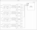
SE617 MTH/HTM CSIG I/O schematic

Interfaces
Clocked Serial Interface (CSI)
The two NEC V850 CPUs on board both support Clocked Serial Interfaces (CSI). All interfaces on the chip are tagged alphabetically, and the CSI interfaces are tagged "G", so the datasheet refers to this as CSIG.
The inverter uses the CSI interface to communicate with the outside world, via Denso SE617 differential transceivers. These convert the single-ended signal line into two signals (a positive and negative version) which is better suited to noise rejection and can be sent outside the inverter.
See Toyota Inverter Clocked Serial Interface Protocol for details on the data sent over these interfaces.