Toyota Prius Gen3 Board: Difference between revisions
No edit summary |
|||
| Line 95: | Line 95: | ||
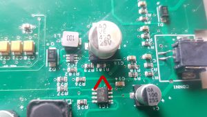
Resistor labeled R101 (labeled '1002') needs swapping for a 8k2 resistor. | Resistor labeled R101 (labeled '1002') needs swapping for a 8k2 resistor. | ||
[[File:20200629 155303.jpg|none|thumb]] | |||
[ | |||
=== Soldering The Breakout Board === | === Soldering The Breakout Board === | ||
Revision as of 14:59, 29 June 2020
The Toyota Prius Gen3 Board is an open source project to repurpose 2010-2015 Toyota Prius inverters for DIY EV use. It consists of a circuit board and programming that replaces the original logic board in the inverter and allows independent control of it without communicating with a Prius ECU.
Note that there is also a Toyota Prius Gen2 Board for the 2004-2009 model years.
Prius Inverter
The Toyota Prius is a hybrid vehicle. Their inverters are suitable and attractive for DIY EVs because of:
- Large part availability. Priuses have been made in large numbers for 20 years.
- High affordability. Prius inverters are available for around $150 from scrapyards everywhere.
- Durability. Toyota engineers appear to have made the inverters foolproof, many inputs and outputs gracefully handle fault conditions.
- Respectable performance. Rated for 50kW output, but tested to handle 600v, and 500+A on MG2. (MG1 unknown, Gen2 had 70% of MG2 on MG1).
- Ease of repurposing. Emulating the original ECU seems reasonably feasible.
The Gen3 Prius (2010-2015 model years) has a variety of useful components inside the inverter package:
- 2 high power inverters, for the 2 motors MG1 (starter) capable of handling 250 amps, and MG2 (drive motor) capable of handling 350 amps.
- A DC-DC converter to provide 12v power supply to the automotive systems and accessories.
- A boost module to boost the 200v battery pack up to 500v, which looks to be able to function as a battery charger (wish list for future development)
- See this video for a thorough disassembly and explanation of the Gen3 Inverter (Timestamp ???? ): https://www.youtube.com/watch?v=Y7Vm-C4MsW8
Control Board
The current version as of Jan 20, 2020 is v2.
As designed by Damien Maguire, the open source hardware for the control board can be purchased as both partially populated and fully populated and tested boards on his website:
Prius Gen3 Prius Gen3 Full & Tested
The control board is a physical replacement for the OEM Prius Gen3 inverter logic board inside the inverter. Remove the old one and replace it with the new one.
Development History
V1 - This board was sold tested but also as a bare logic board requiring purchase of your own components and SMD placement and soldering skills. https://www.evbmw.com/index.php/evbmw-webshop/toyota-bare-boards/prius-gen-3-inverter-bare-logic-board
V2 - A new board source was found to be both high quality and low cost. The boards were redesigned around the inventory of parts available from this supplier. In particular the high cost of populated and soldered boards (10x the price) from the source used to make the v1 boards is so significantly lower on the v2 that there are likely no savings by building and soldering the board yourself. The circuit now has hardware to support repurposing the MG1 inverter as a battery charger, though as of Jan 20, 2020, software is still in development.
Vendors
- ?? List of known vendors with support?
Support
Community support is available on the Prius Gen 3 Inverter Logic Board Support Thread
You are not entitled to support, purchase from a vendor who offers support if you want it guaranteed. Treat the community with respect.
Inverter Model Numbers
| Inverter No | Car model(s) | Logic Board No | Power Board No | Compatible 50 pin connector | PCB size | Confirmed works with board | Link |
|---|---|---|---|---|---|---|---|
| G9200-47141 | Auris 2012, RHD | ||||||
| G9200-47140 | Prius 2010 | F1759-47041 01 | |||||
| G9200-47180 | Photo diyelectriccar.com | ||||||
| G9200-47190 | Auris | F1759-52010 04 | ? | Forum Thread openinverter.com | |||
| G9200-52010 | Yaris | F1759-52010 04 | F1789-52010 | 154x143mm | https://openinverter.org/forum/viewtopic.php?f=14&t=257&p=5828#p5828 | ||
| G9200-52032 | Yaris 2015 | F1759-52010 04 | F1789-52010 | YES | Long 143mm | Forum Thread openinverter.com Forum Thread openinverter.com | |
| G9201-52011 | Yaris | YES | Forum Thread openinverter.com | ||||
| G9201-52012 | Prius C | F1759-52010 | F1789-52010 | YES (presumably) | Forum Thread openinverter.com |
Kit Assembly Instructions (V1C)
This guide is for the assembly of version V1C of the Gen 3 board available here: https://www.evbmw.com/index.php/evbmw-webshop/toyota-built-and-tested-boards/prius-gen-3-inverter-built-tested
This is based on the assembly videos by Damien Maguire.
Part 1: https://www.youtube.com/watch?v=QE-zym8iIgM&t=2643s
Part 2: https://www.youtube.com/watch?v=Nu5_OBOPk4s&t=1787s
Early Board Correction, pre July 2020
The first batch of JLCPCB boards shipped have an incorrect resistor value that needs to be changed over. Boards shipped after Jun 26, 2020 will not need to do this.
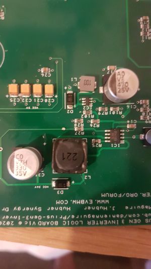
Resistor labeled R101 (labeled '1002') needs swapping for a 8k2 resistor.
Soldering The Breakout Board
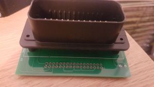
Solder the Ampseal socket to the the breakout board, the silk-screen indicates side and orientation fitment.
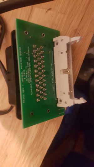
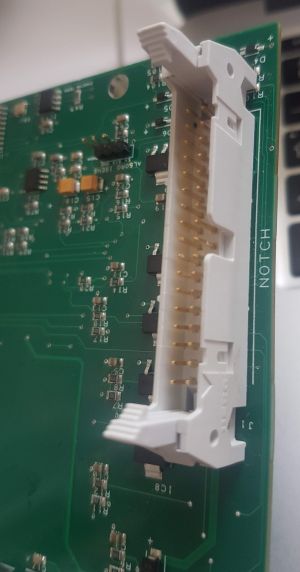
Next flip it over and solder the 34 way IDC locking header on, notch upwards as show.
Note: Some versions of the breakout board have and error in the silk-screen that indicate orientation incorrectly, with the notch towards the bottom.
Soldering the Main Board
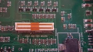
The main board is mostly pretty easy to solder, the one exception is the 50 way white connector. I found that putting flux on the pads and dragging solder across them, placing the connector in place and then placing the iron on the pins was the easiest.
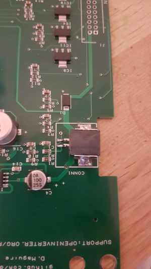
Next up I did conn 1, it can only go one way, and is a piece of cake after the 50 way connector.
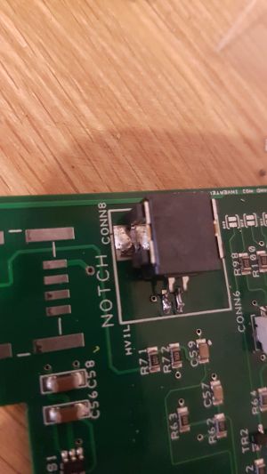
And Conn8, again easy.
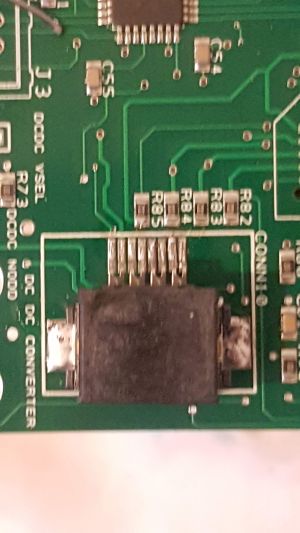
Next the DCDC convert connector, again only fits one way.
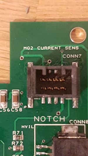
MG1 and MG2 Current sensor Connectors, both these are the same, the tabs on both MG1 and MG2 are at the top.
Next up the L2 inductor, it can go either way
Next up I did the right angled pins for the wifi module, stick the pins in the module connector and then through the board, hold it in place and flip it over.
[add photo]
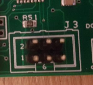
Cut 2 lengths of 3 pins from the header pin strips for the ISP header for programming the Atmega328P that will be used ton control the buck-boost converter.
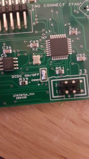
To enable the DCDC converter for I've bridged over the 2 pin holes, but you can add a switch or something here, or leave it open if you're not using the DCDC to keep the 12v battery charged.
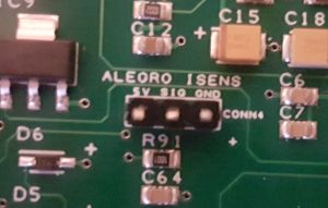
Pin header for Alegro current sensor, currently no software exists to control the buck boost, hopefully in the future this will be able to be used as a charger, this pin header is for the possible addition of a current sensor to facilitate.
Next, cut 3 pin headers and 6 pin headers off the strip, the 3 are for the single wire program interface for the STM32, the 6 is for x
Last up is the lock connector for the breakout board. Notch outward.
Powering up
Now it's time to power up the board with 12v and test.
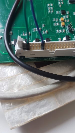
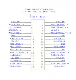
Green wire is +12v (pin 1) and blue 0v (pin 11)
Checking voltages
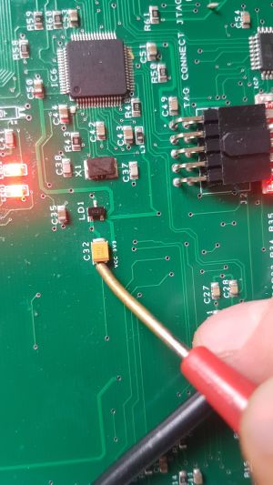
Check for ~3.3v here on C32
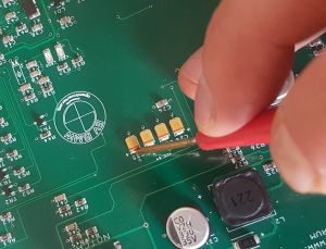
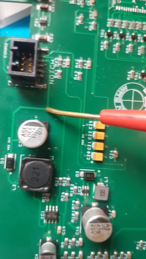
Check for ~5v here on C21/C20/C22/C25
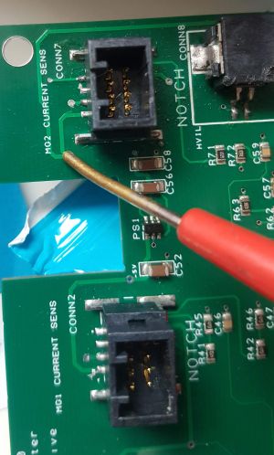
Check for -5v here on the little via next to CONN7 or right next to CONN2 there's a via with -5V under it.
Finally the 26v
Firmware
Wifi Module Firmware
My wifi module came with the firmware already installed, but if yours didn't follow the steps below.
Main Firmware
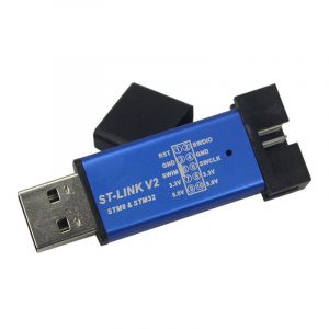
There's many ways of achieving this but this is what I did, using an STLink V2 clone available on eBay for a couple of £.
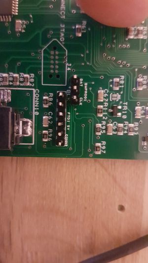
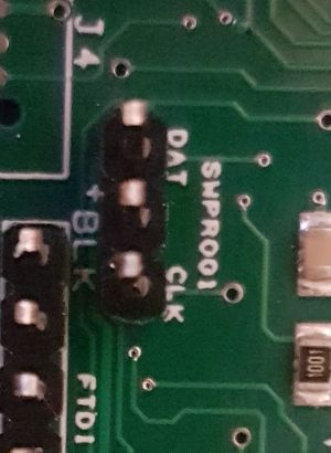
Connect the 3 wire pin headers to the programming device.
The pin labeled DAT on the board should connect to SWDIO
The middle pin of the 3 pins on the board should go to GND on the STLink V2
The pin labeled CLK on the board should connect to SWCLK
Using a Mac or Linux install https://github.com/stlink-org/stlink
Run command to write the bootloader
st-flash write stm32_loader.bin 0x08000000
For Windows
[Add instructions for writing bootloader]
Once the bootloader has been programmed the main firmware can be uploaded and upgraded via the web interface.
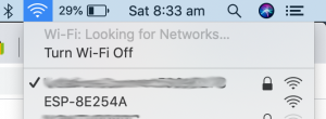
A wifi network should be visible with the name ESP-* connect to it
Once connected open a browser and navigate to http://192.168.4.1 and find the update section, upload the firmware.
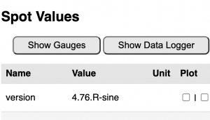
Once this has completed you can verify by scrolling to the Spot Values section and you'll see the software version
Atmega328p Firmware
This will control the Buck Boost module that's hopefully going to be a functioning charger in the future, it also requires a simple bit of firmware to enable the DC-DC converter.
[Add instructions for firmware]
DC-DC Converter
The inverter contains a DC DC converter, that is used to keep the 12v battery charged using the high voltage battery. This is the EV equivalent to the alternator on a combustion engined car.
As per the assembly instructions above this needs to be enabled via the jumper on the control board.
In the unmodified state, the DC DC converter will operate with a main battery voltage in the ~80v to ~235v range and will require a simple modification to allow it to operate at higher voltage range, ~140v to ~400v
[instructions for modification to follow]
12v Battery Connection
[Add details]
High Voltage Battery Connection
[Add battery connection details]
Ampseal Socket & Plug
There are two part numbers for the large 35 way Ampseal through hole socket
TE Connectivity 1-776163-1 (black) or 1-776163-4 (grey)
There are numerous part numbers for the mating Free Hanging Plug Housing, the most common and affordable is:
TE Connectivity 776164-2
Connecting Resolver
For resolver connect EXC to one side of the exciter winding and other to Ground.
Connect one side of SIN winding to SIN and other to Encoder A
Conenct one side of COS winding to COS and other to encoder B.
Notes
Bill of Materials (from above)
The control board takes advantage of the OpenInverter.org software for control.


